PS2 keyboard controller
PS2 keyboard protocol uses two serial signals. Note that ps2_clk cannot be used directly as a clock signal.

PS2 keyboard controller:

The following Verilog HDL code implements the PS2 keyboard controller.
1 2 3 4 5 6 7 8 9 10 11 12 13 14 15 16 17 18 19 20 21 22 23 24 25 26 27 28 29 30 31 32 33 34 35 36 37 38 39 40 41 42 43 44 45 46 47 48 49 50 51 52 |
// PS2 keyboard interface, by Li Yamin, yamin@ieee.org module ps2_keyboard (clk,clrn,ps2_clk,ps2_data,rdn,data,ready,overflow); input clk, clrn; // 50 MHz input ps2_clk; // ps2 clock input ps2_data; // ps2 data input rdn; // read, active low output [7:0] data; // 8-bit code output ready; // code ready output reg overflow; // fifo overflow reg [9:0] buffer; // ps2_data bits reg [7:0] fifo[7:0]; // circular fifo reg [3:0] count; // count ps2_data bits reg [2:0] w_ptr,r_ptr; // fifo w/r pointers reg [3:0] ps2_clk_sync; // for detecting falling edge always @ (posedge clk) ps2_clk_sync <= {ps2_clk_sync[2:0],ps2_clk}; // shift ps2_clk left wire sampling = ps2_clk_sync[3] & // 1 ps2_clk_sync[2] & // 1 ~ps2_clk_sync[1] & // 0 ~ps2_clk_sync[0]; // 0: had a falling edge always @ (posedge clk) begin if (!clrn) begin // on reset count <= 0; // clear count w_ptr <= 0; // clear w_ptr r_ptr <= 0; // clear r_ptr overflow <= 0; // clear overflow end else if (sampling) begin // if sampling if (count == 4'd10) begin // for one frame if ((buffer[0] == 0) && // start bit (ps2_data) && // stop bit (^buffer[9:1])) begin // odd prity if ((w_ptr + 3'b1) != r_ptr) begin fifo[w_ptr] <= buffer[8:1]; w_ptr <= w_ptr + 3'b1; // w_ptr++ end else begin overflow <= 1; // overflow end end count <= 0; // for next frame end else begin // else buffer[count] <= ps2_data; // store ps2_data count <= count + 4'b1; // count++ end end if (!rdn && ready) begin // on cpu read r_ptr <= r_ptr + 3'b1; // r_ptr++ overflow <= 0; // clear overflow end end assign ready = (w_ptr != r_ptr); // fifo is not empty assign data = fifo[r_ptr]; // code byte endmodule |
Display keyboard key's scan codes on VGA
When you press the key 'L', the keyboard controller will give you its scan code consisting of three bytes 0x4b, 0xf0, and 0x4b. The first 0x4b is called make code and 0xf0 and 0x4b is the break code. The keyboard controller sends these three bytes one by one. If the ready signal issued by the keyboard controller is a one, you can get one byte. Then you must send an active-low rdn to inform the keyboard controller.

To display the value of a byte on the display, you need to convert it to two ASCII characters. For example, the byte 0x4b will be translated to 0x34 (the ASCII 0f 4) and 0x62 (the ASCII 0f b). Then you can write these two ASCII characters to the character RAM. After a character was written into the character RAM, the RAM address must be increased by a one.

1 2 3 4 5 6 7 8 9 10 11 12 13 14 15 16 17 18 19 20 21 22 23 24 25 26 27 28 29 30 31 32 33 34 35 36 37 38 39 40 41 42 43 44 45 46 47 48 49 50 51 52 53 54 55 56 57 58 59 60 61 62 63 64 65 66 67 68 69 70 71 72 73 74 75 76 77 78 79 80 81 82 83 84 85 86 87 88 89 90 91 92 93 94 95 96 97 98 99 100 101 102 103 104 105 106 107 108 109 110 111 112 113 114 115 116 117 118 119 120 121 122 123 124 125 126 127 128 129 130 131 132 133 134 135 136 137 138 139 140 141 142 143 144 145 146 147 148 149 150 151 152 153 |
// Display keyboard's scan code on display without using cpu, by Li Yamin // // Single-port char ram +-posedge stores VGA address for read // | +-posedge stores kbd ascii to char ram // _____ _____ |_____ |_____ _____ _____ // sys_clk |_____| |_____| |_____| |_____| |_____| |_____| | // (50mhz) +-negedge | | VGAC | keyboard | | | // | generates | | reads | writes | | | // | clk25m | | char ram | char ram | | | // | | | | we&~clk25m| | | // |___________| |___________| |___________| | // clk25m | |___________| |___________| |___________| // +-posedge +-negedge | // | VGAC | registers | // | outputs | ascii | // clk25m is used as the selection | address | for VGA | // signal of multiplexer for ram |------ one cycle ------| // kbd _______________________ // ready |_______________________| |_______________________| // _______________________ // key_byte -----------------------|_______________________|------------------------ // ___________________________________ ___________ // io_rdn |_______________________| module display_scan_code_without_space (sys_clk,clrn,ps2_clk,ps2_data,r,g,b,hs,vs); input sys_clk,clrn; input ps2_clk,ps2_data; output [3:0] r,g,b; // red, green, blue colors, 4-bit for each output hs,vs; // horizontal and vertical synchronization // output of char ram wire [6:0] ascii; // output of char ram reg [6:0] ascii_reg; // registered ascii // signals for writing keyboard ascii to char ram reg kbd_wmem; // char ram write enable reg io_rdn; // keyboard read reg [12:0] ram_w_addr = 13'h0; // signals for vgac and font table wire [8:0] row_addr; // vga pixel row address, 480 (512) lines wire [9:0] col_addr; // vga pixel col address, 640 (1024) pixels wire rdn; // read pixel ram (active low), not used wire ft_dot; // font dot wire [11:0] vgac_din = (ft_dot) ? 12'hfff : 12'h00f; // rrrr_gggg_bbbb, pixel wire [5:0] char_row = row_addr[8:3]; // char row wire [6:0] char_col = col_addr[9:3]; // char col wire [12:0] ft_addr = {ascii_reg,row_addr[2:0],col_addr[2:0]}; // font_table address wire [12:0] vga_addr = {char_row,6'h0} + {char_row,4'h0} + char_col; // row*(64+16)+col // clock 25mhz reg clk25m = 1; // clk25m: 25MHz always @(negedge sys_clk) begin clk25m <= ~clk25m; // clk25m: 25MHz end // register ascii for access to font table always @(negedge clk25m) begin ascii_reg <= ascii; // registered ascii end // vgac vgac vc (clk25m,clrn,vgac_din,row_addr,col_addr,rdn,r,g,b,hs,vs); // vgac // char ram, 80 * 60 = 4800, posedge writes data and stores address for read wire [12:0] ram_addr = clk25m ? vga_addr : ram_w_addr; // ram read : ram write wire ram_we = kbd_wmem & ~clk25m; // ram write enable wire [6:0] ram_din; // ascii, 7-bit, to be written char_ram cr (sys_clk,ram_addr,ascii,ram_din,ram_we); // single-port ram // font_table 128 x 8 x 8 x 1 font_table ft (ft_addr,ft_dot); // ps2_keyboard wire [7:0] key_byte; reg [7:0] key_byte_reg; wire ready,overflow; ps2_keyboard kbd (clk25m,clrn,ps2_clk,ps2_data,io_rdn,key_byte,ready,overflow); // update char ram address and index reg two_ascii_index = 0; // 0, 1 assign ram_din = get_one_ascii(two_ascii_index); always @ (negedge clk25m) begin if (kbd_wmem) begin two_ascii_index <= ~two_ascii_index; ram_w_addr <= ram_w_addr + 13'd1; end end // read keyboard and write char ram always @ (negedge clk25m) begin if (ready) begin key_byte_reg <= key_byte; // register scancode kbd_wmem <= 1; // write 2-ascii to char ram io_rdn <= 0; // read keyboard end else begin if (two_ascii_index == 1) kbd_wmem <= 0; io_rdn <= 1; end end // w w // __ __ |__ __ |__ __ __ __ __ __ __ // sys_clk |__| |__| |__| |__| |__| |__| |__| |__| |__| |__| |__| | // kbd ___________ // ready ________| |________________________________________________ // _ _____ w _____ w _____ _____ _____ // clk25m |_____| r |_____| r |_____| r |_____| r |_____| r |_____| // _____________________________________________________ // key_byte_reg --------|_____________________________________________________ // _______________________ // kbd_wmem ____________| |_____________________________ // _____________________________________________________ // two_ascii_index |_0_________|_1_________|_0___________________________ // | | // write 1st write 2nd // ______________ _________________________________________ // io_rdn |___________| // // get one ascii from two function [6:0] get_one_ascii; input index; case (index) 'd0: get_one_ascii = bin2ascii(key_byte_reg[7:4]); 'd1: get_one_ascii = bin2ascii(key_byte_reg[3:0]); endcase endfunction // binary to ascii function [6:0] bin2ascii; input [3:0] binary; case (binary) 'h0: bin2ascii = 7'h30; // 0 'h1: bin2ascii = 7'h31; // 1 'h2: bin2ascii = 7'h32; // 2 'h3: bin2ascii = 7'h33; // 3 'h4: bin2ascii = 7'h34; // 4 'h5: bin2ascii = 7'h35; // 5 'h6: bin2ascii = 7'h36; // 6 'h7: bin2ascii = 7'h37; // 7 'h8: bin2ascii = 7'h38; // 8 'h9: bin2ascii = 7'h39; // 9 'ha: bin2ascii = 7'h61; // a 'hb: bin2ascii = 7'h62; // b 'hc: bin2ascii = 7'h63; // c 'hd: bin2ascii = 7'h64; // d 'he: bin2ascii = 7'h65; // e 'hf: bin2ascii = 7'h66; // f endcase endfunction endmodule |
Exercise
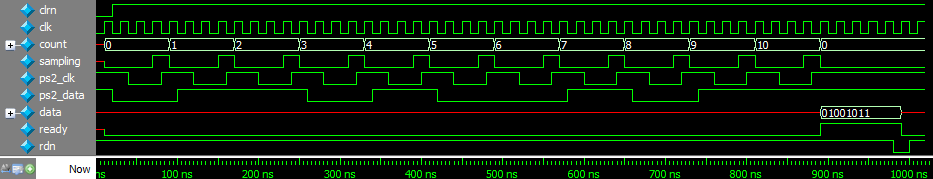
- Write a test bench ps2_keyboard_tb.v for ps2_keyboard.v to get the following waveform.
- In order to see the value clearly, append a SPACE (ASCII 0x20) to each byte value (two ASCII characters) on the display.
That is, we display three ASCII characters on the display for one byte of the scan code. For example, change display from
124bf04bf012
to12 4b f0 4b f0 12
You can use a signal three_ascii_index which is the index of the three ASCII characters (index value: 0, 1, 2). After a character was written into the character RAM, the index must be increased by a one. Note that for the index, 2 + 1 will become 0.
Implement it on FPGA. You can download the following Verilog HDL codes.
- ps2_keyboard.v (keyboard controller)
- vgac.v (VGA controller)
- char_ram.v (data memory - character RAM)
Pin assignments:
set_location_assignment PIN_M9 -to sys_clk
set_location_assignment PIN_P22 -to clrn
set_location_assignment PIN_B6 -to b[0]
set_location_assignment PIN_B7 -to b[1]
set_location_assignment PIN_A8 -to b[2]
set_location_assignment PIN_A7 -to b[3]
set_location_assignment PIN_L7 -to g[0]
set_location_assignment PIN_K7 -to g[1]
set_location_assignment PIN_J7 -to g[2]
set_location_assignment PIN_J8 -to g[3]
set_location_assignment PIN_A9 -to r[0]
set_location_assignment PIN_B10 -to r[1]
set_location_assignment PIN_C9 -to r[2]
set_location_assignment PIN_A5 -to r[3]
set_location_assignment PIN_H8 -to hs
set_location_assignment PIN_G8 -to vs
set_location_assignment PIN_D3 -to ps2_clk
set_location_assignment PIN_G2 -to ps2_data
- (Option) Implement and simulate the circuits described in the paper https://ieeexplore.ieee.org/document/563604. If you are off campus, use Hosei VPN to download the PDF.
- (Option) Implement and simulate the circuits described in the paper https://ieeexplore.ieee.org/document/7546386. If you are off campus, use Hosei VPN to download the PDF.