Overview of design flow
- Build a project
- Project name and location
- Project Verilog HDL files (.v)
- Project constraint file (.xdc)
- Project device (Zynq-7000 xc7z020clg400-1)
- Functional simulation
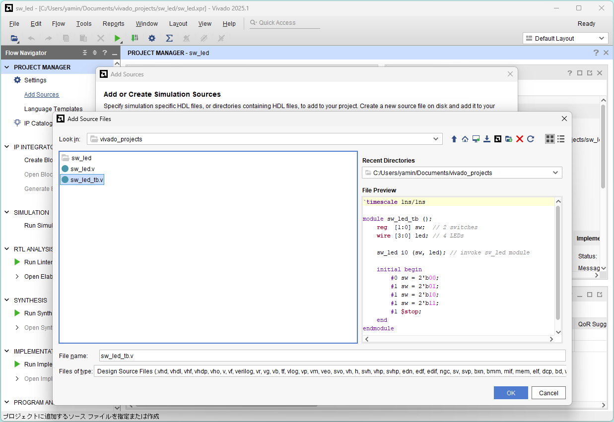
- Project testbench file (_tb.v)
- Run simulation
- Check and save waveform file
- Run synthesis
- Run implementation
- Generate bitsteam
- Program device
Build a project
Create a folder C:\Users\admin\Documents\vivado_projects
Prepare the following three files in the folder.
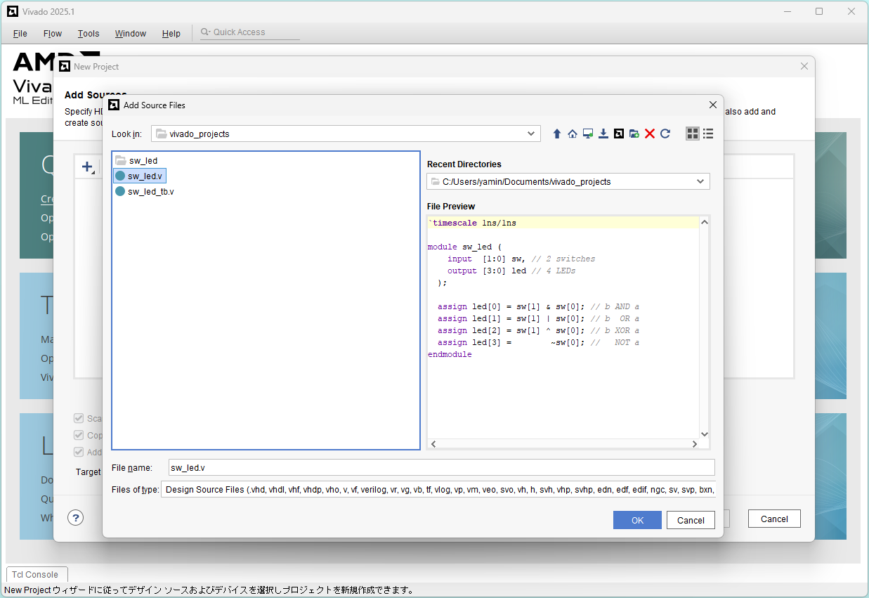
- A circuit sw_led.v
`timescale 1ns/1ns module sw_led ( input [1:0] sw, // 2 switches output [3:0] led // 4 LEDs ); assign led[0] = sw[1] & sw[0]; // b AND a assign led[1] = sw[1] | sw[0]; // b OR a assign led[2] = sw[1] ^ sw[0]; // b XOR a assign led[3] = ~sw[0]; // NOT a endmodule - A test bench sw_led_tb.v
`timescale 1ns/1ns module sw_led_tb (); reg [1:0] sw; // 2 switches wire [3:0] led; // 4 LEDs sw_led i0 (sw, led); // invoke sw_led module initial begin #0 sw = 2'b00; #1 sw = 2'b01; #1 sw = 2'b10; #1 sw = 2'b11; #1 $stop; end endmodule - A constraint (pin assignment) pynq-z2.xdc
##Switches

set_property -dict { PACKAGE_PIN M20   IOSTANDARD LVCMOS33 } [get_ports { sw[0] }]; #IO_L7N_T1_AD2N_35 Sch=sw[0]
set_property -dict { PACKAGE_PIN M19   IOSTANDARD LVCMOS33 } [get_ports { sw[1] }]; #IO_L7P_T1_AD2P_35 Sch=sw[1]

##LEDs

set_property -dict { PACKAGE_PIN R14   IOSTANDARD LVCMOS33 } [get_ports { led[0] }]; #IO_L6N_T0_VREF_34 Sch=led[0]
set_property -dict { PACKAGE_PIN P14   IOSTANDARD LVCMOS33 } [get_ports { led[1] }]; #IO_L6P_T0_34 Sch=led[1]
set_property -dict { PACKAGE_PIN N16   IOSTANDARD LVCMOS33 } [get_ports { led[2] }]; #IO_L21N_T3_DQS_AD14N_35 Sch=led[2]
set_property -dict { PACKAGE_PIN M14   IOSTANDARD LVCMOS33 } [get_ports { led[3] }]; #IO_L23P_T3_35 Sch=led[3]
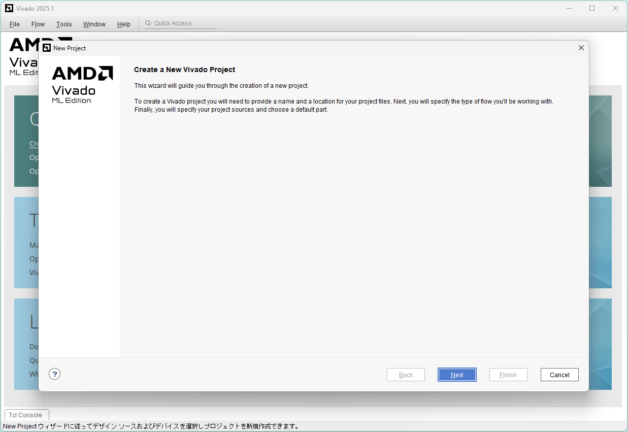
Start Vivado and click Create Project >
Click Next
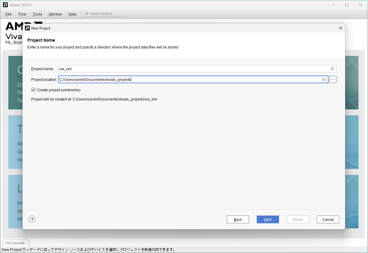
Input Project name and Project location, and click Next
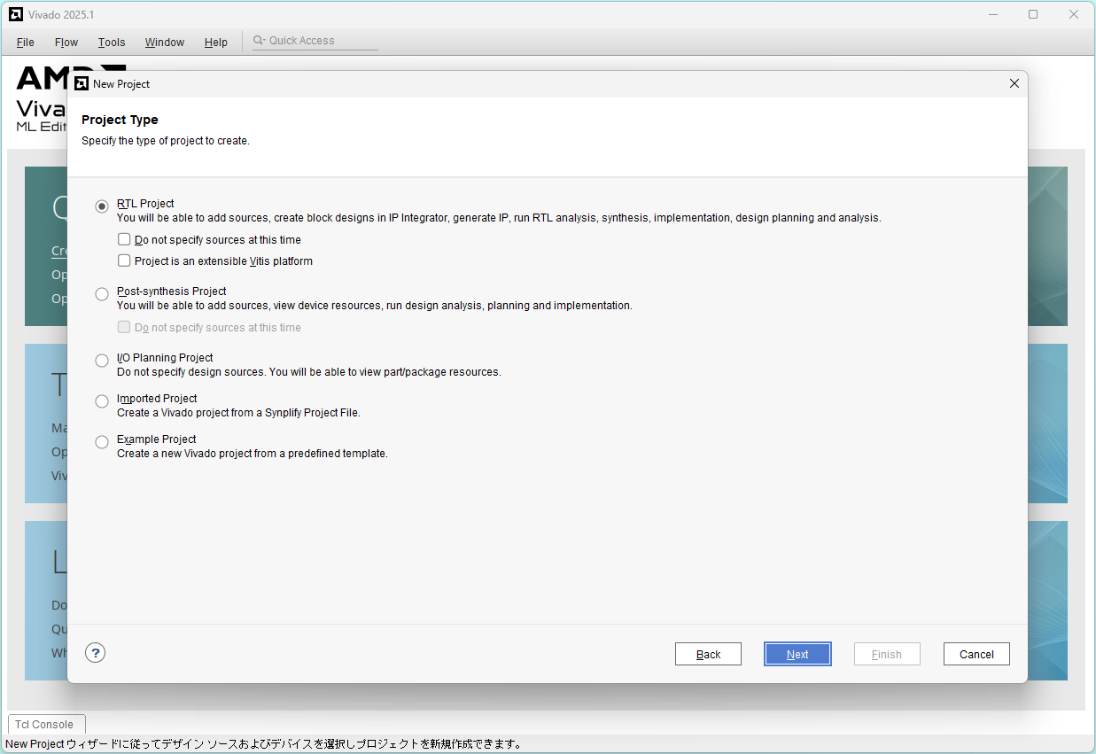
Select RTL Project and click Next
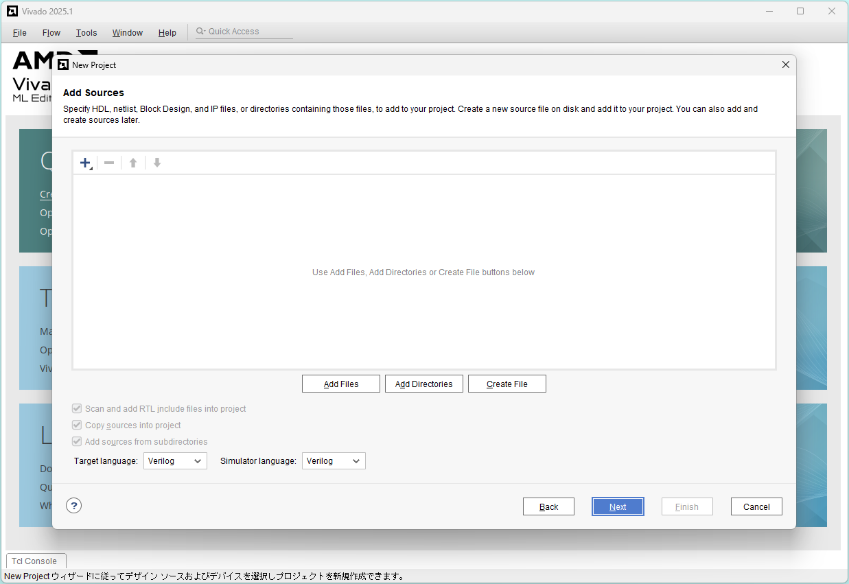
Click Add Files
Select sw_led.v and click OK
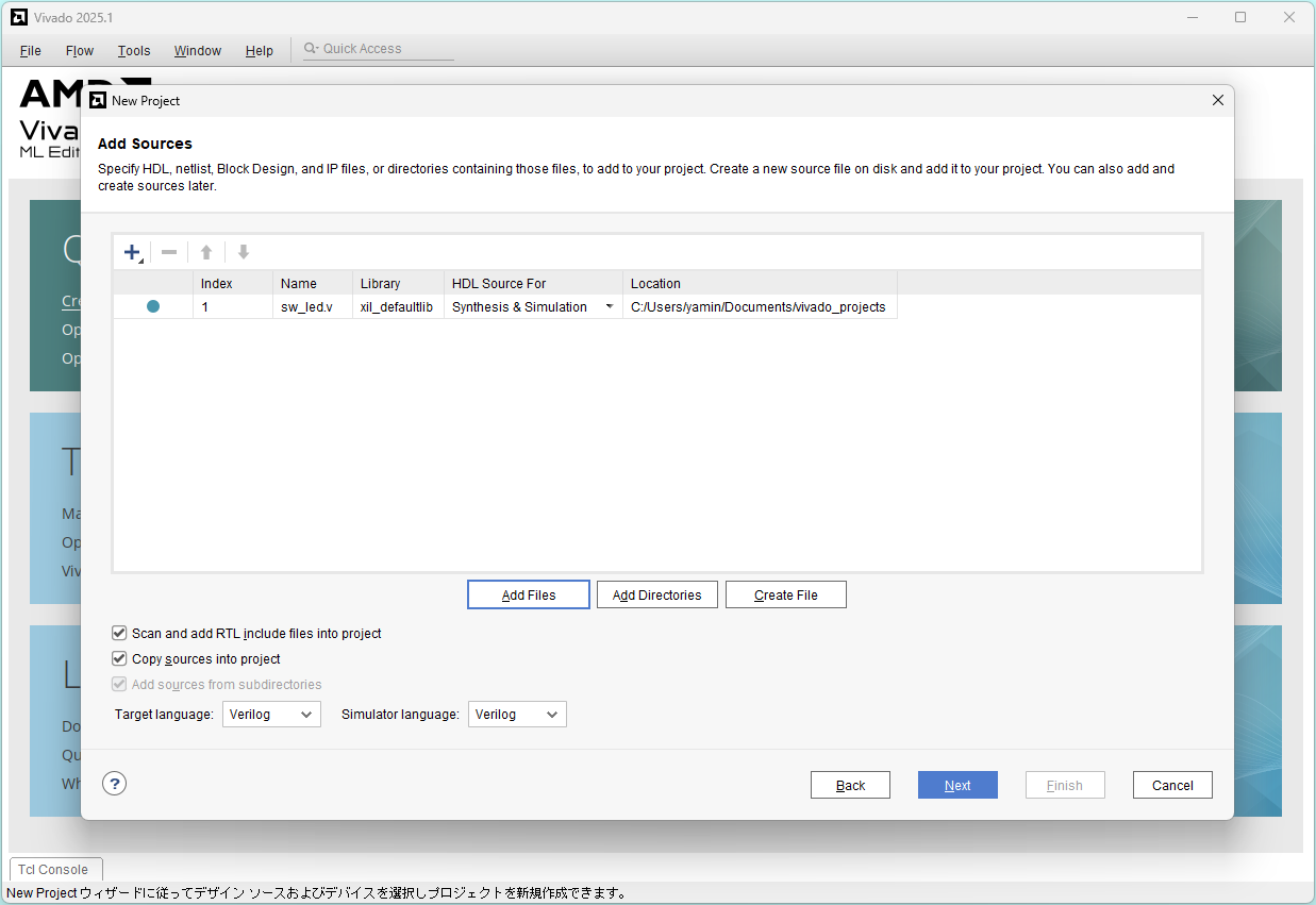
Uncheck "Scan..." and "Copy..." and Click Next
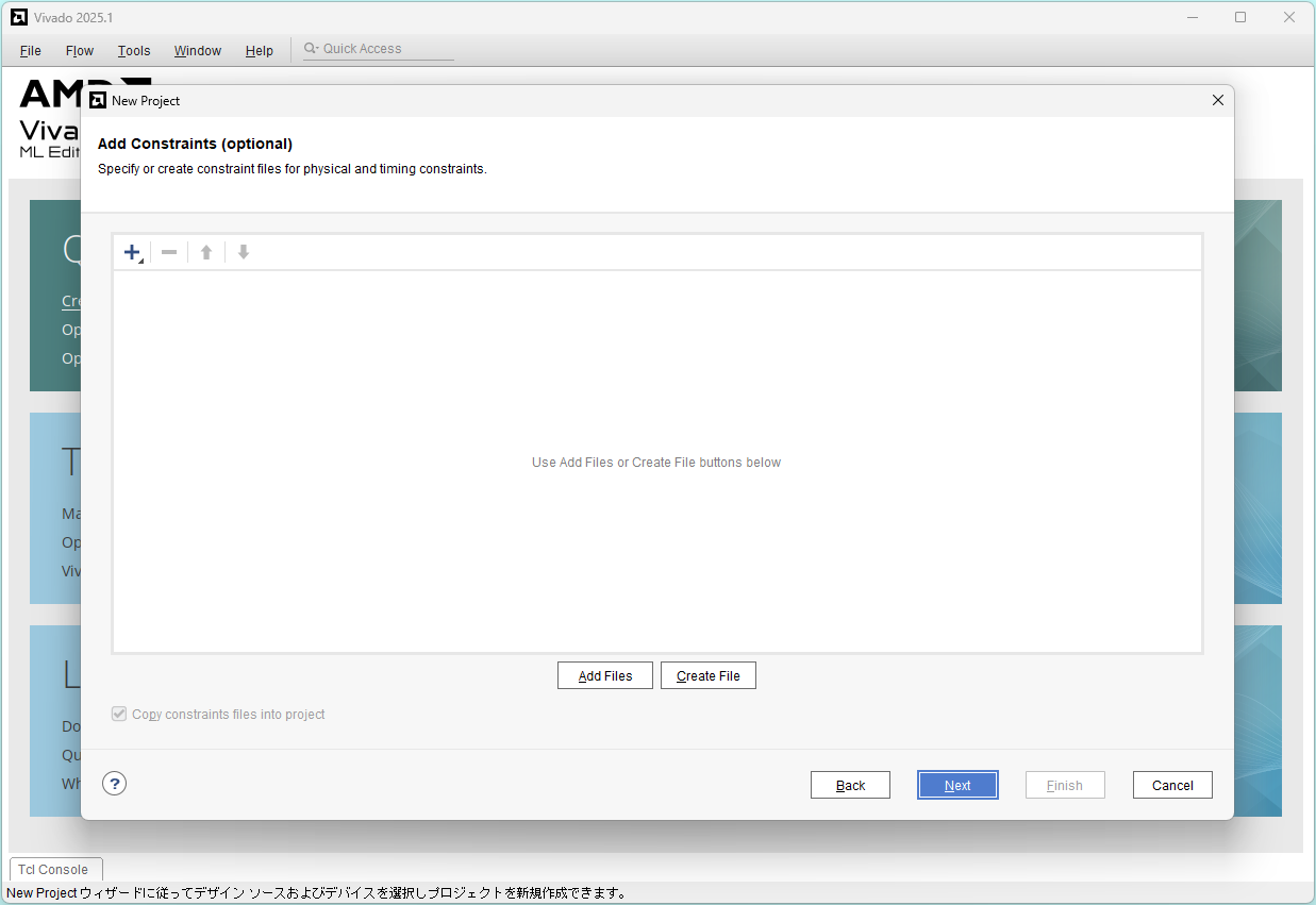
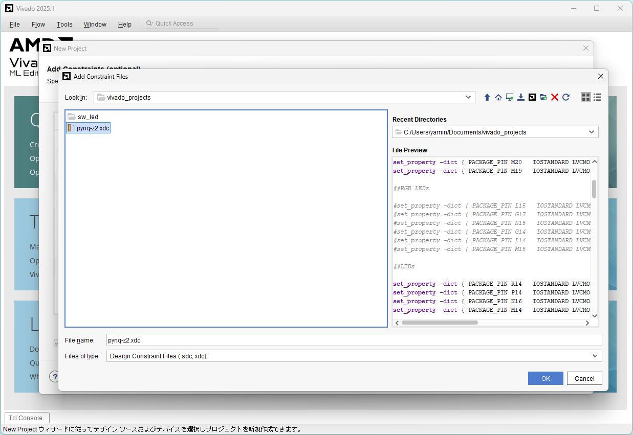
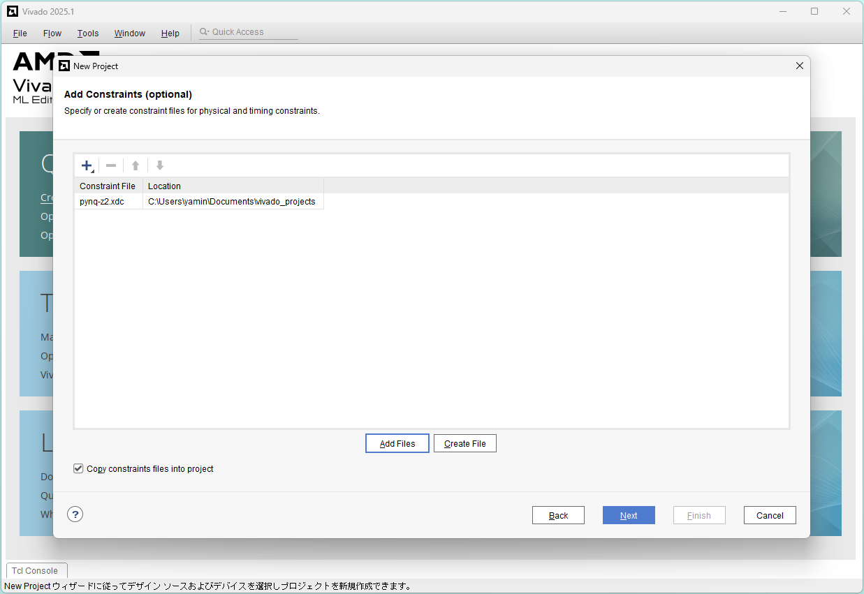
Add Constraints: Click Add Files
Select pynq-z2.xdc and click OK
Uncheck "Copy..." and Click Next
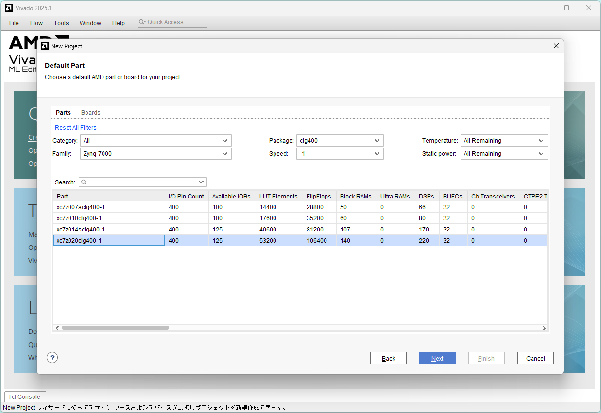
Choose Zynq-7000 clg400-1 part: xc7z020clg400-1, and click Next
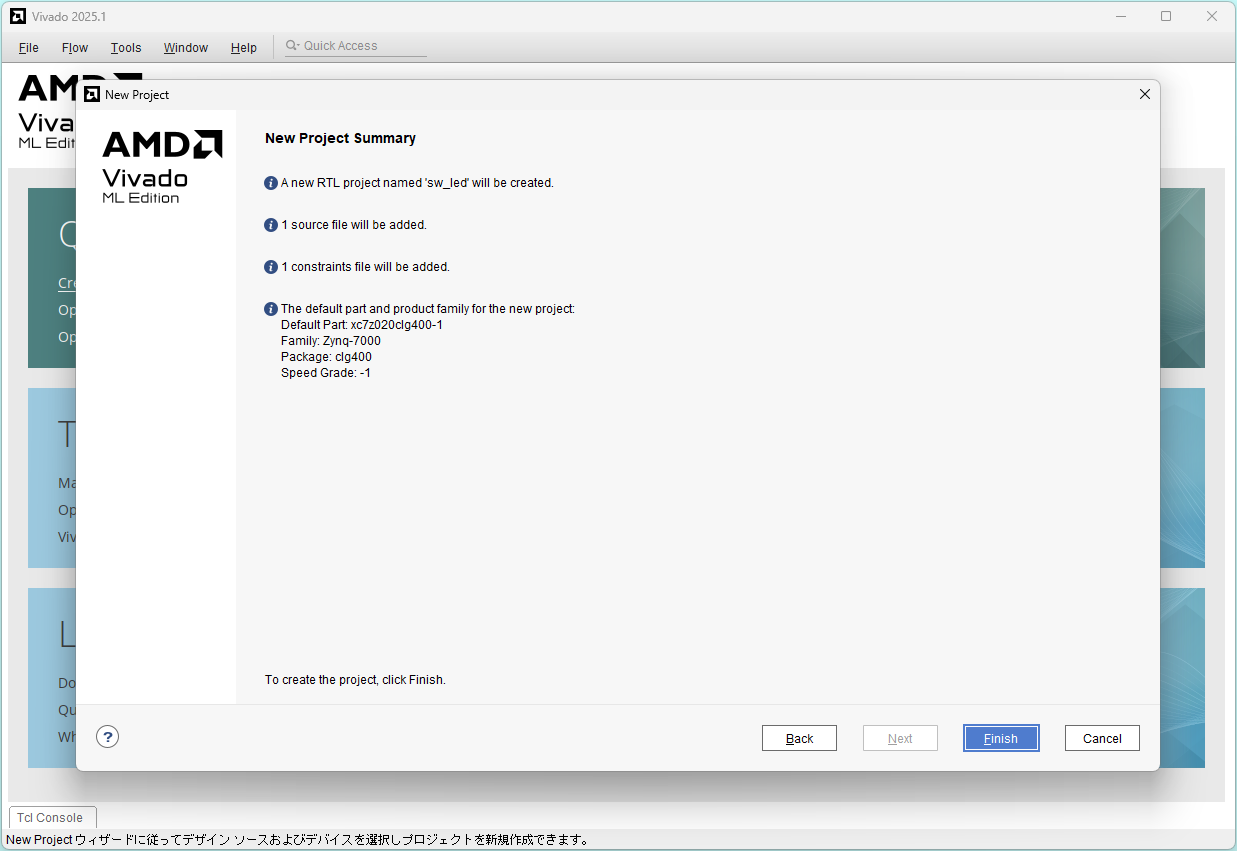
Project summary: Click Finish
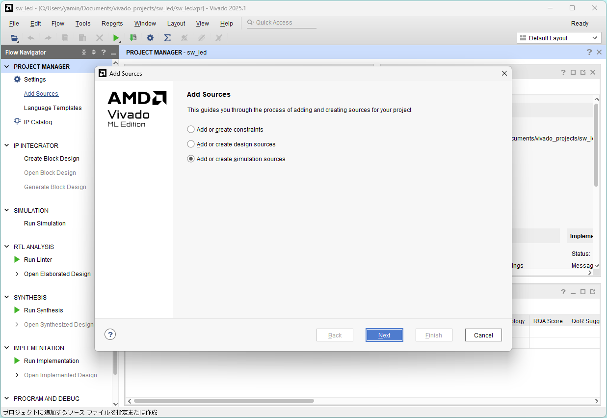
Functional simulation
Click Add Sources and select Add or create simulation sources, and click Next
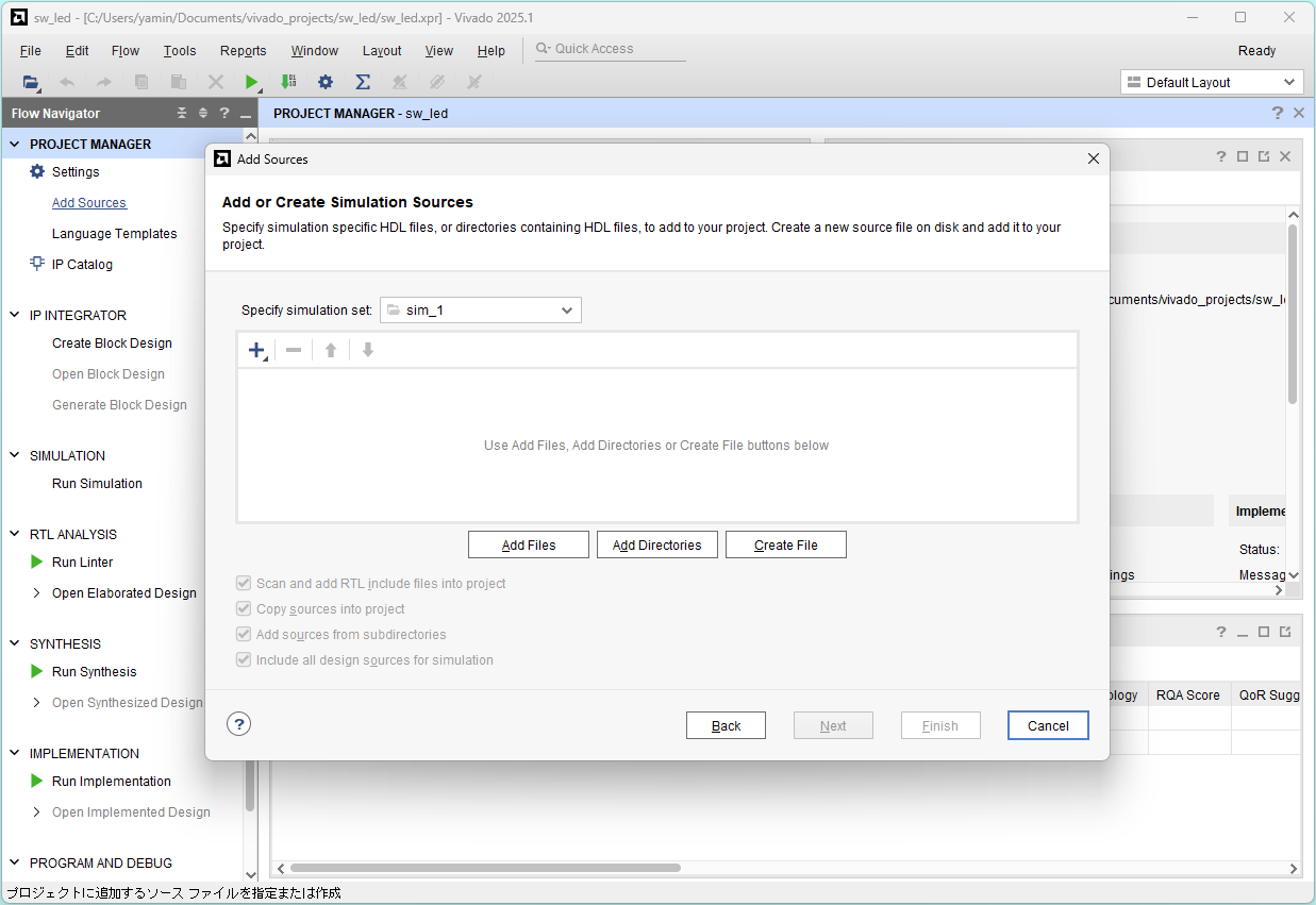
Click Add Files
Select sw_led_tb.v and click OK
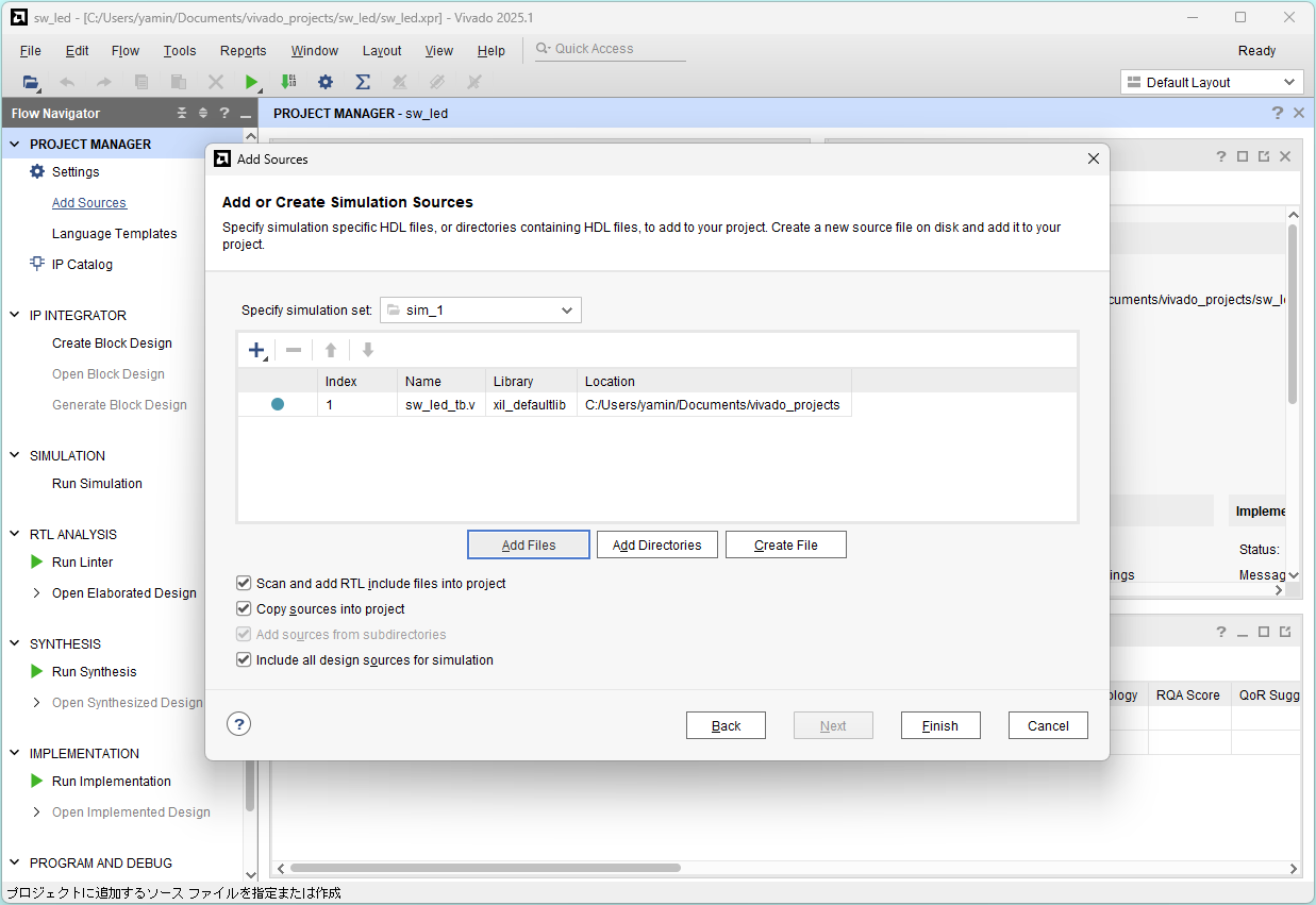
Click Finish
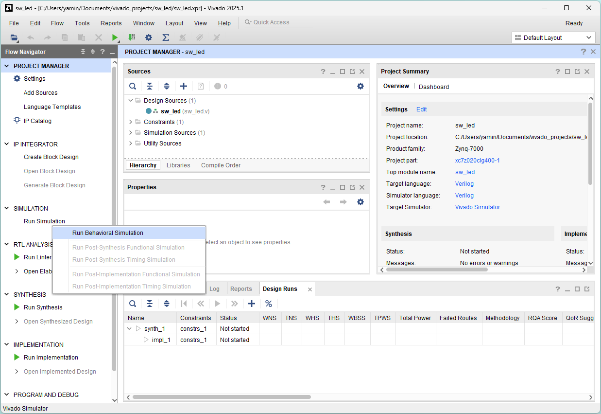
Click Run Simulation and Run Behavioral Simulation
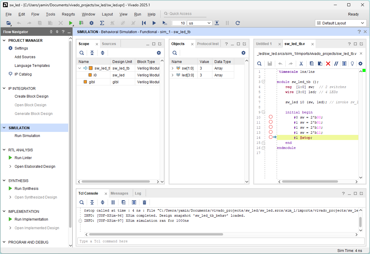
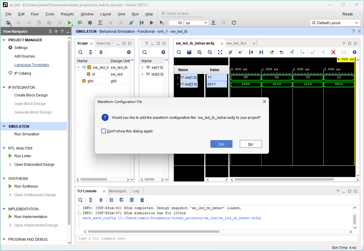
Simulation finished
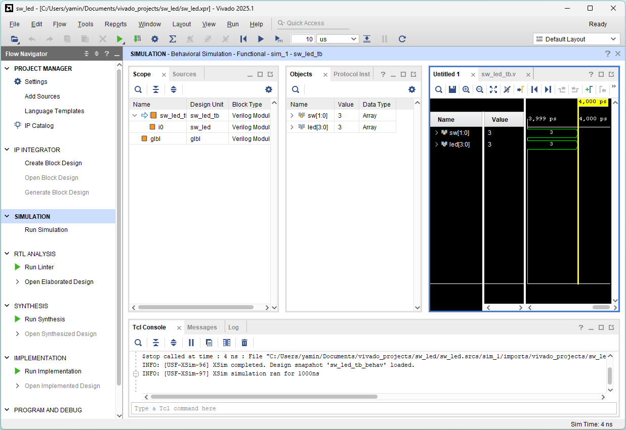
Select Untitled 1 window (waveform)
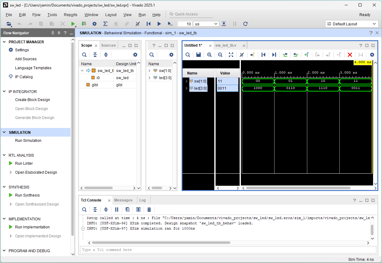
Adjust waveform window and choose Binary Radix for signals
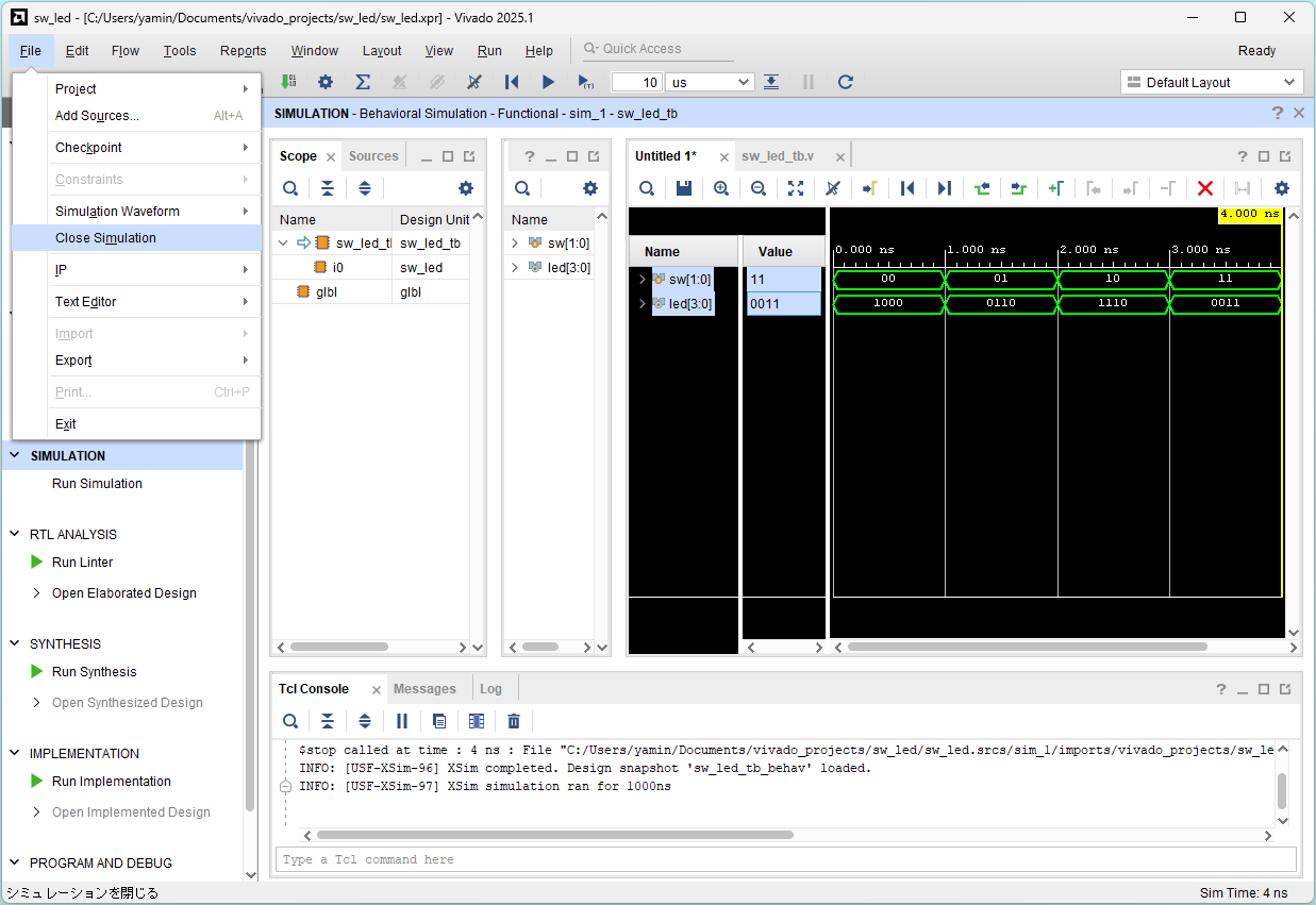
Check the correctness:
 sw[1:0] = 00   01   10   11
led[3:0] = 1000 0110 1110 0011
           ||||
           |||+--- sw[1] & sw[0]
           ||+---- sw[1] | sw[0]
           |+----- sw[1] ^ sw[0]
           +------------- ~sw[0]
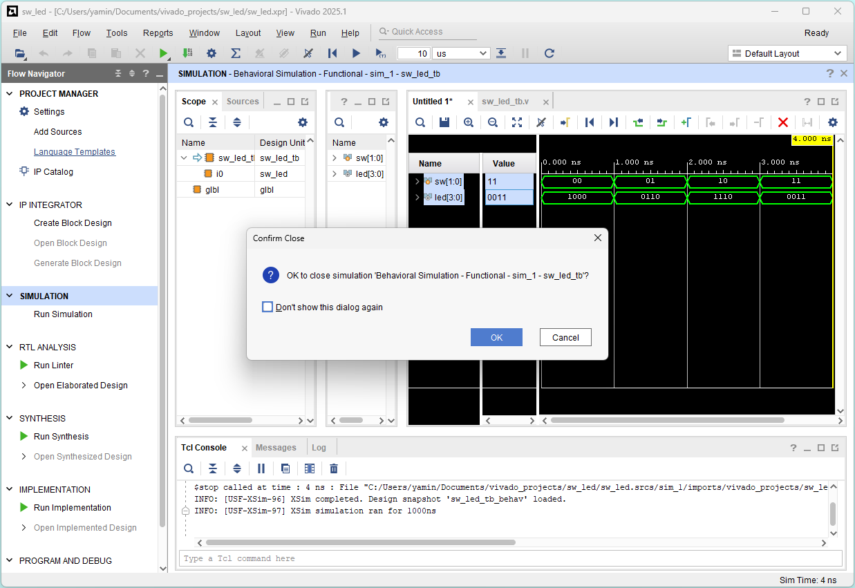
File - Close Simulation
Click OK
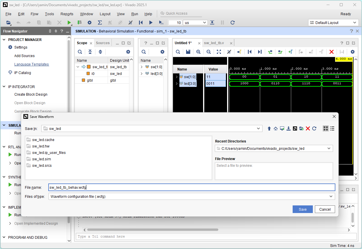
Click Save
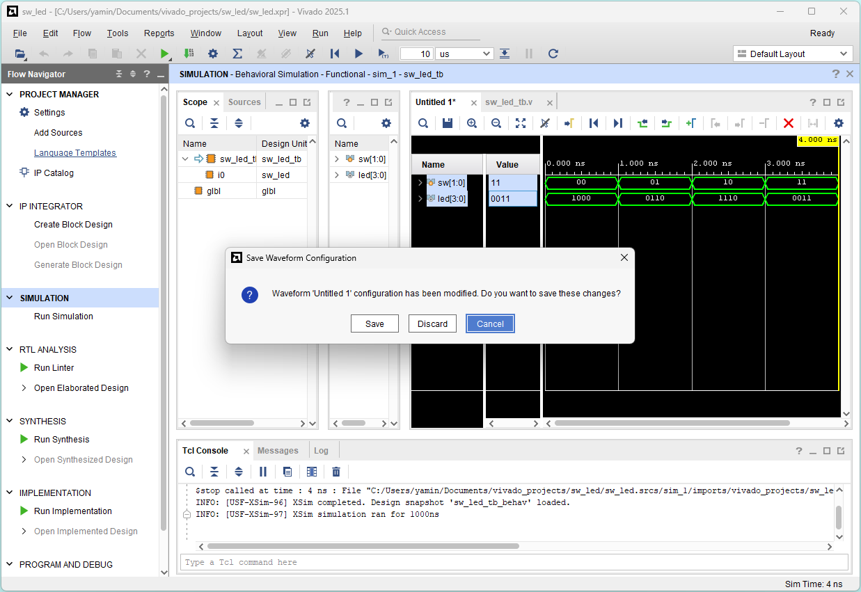
Click Save
Click Yes
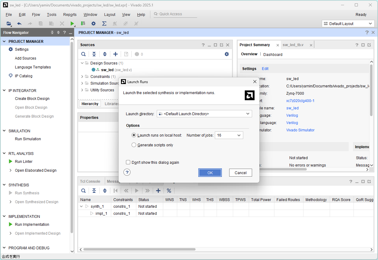
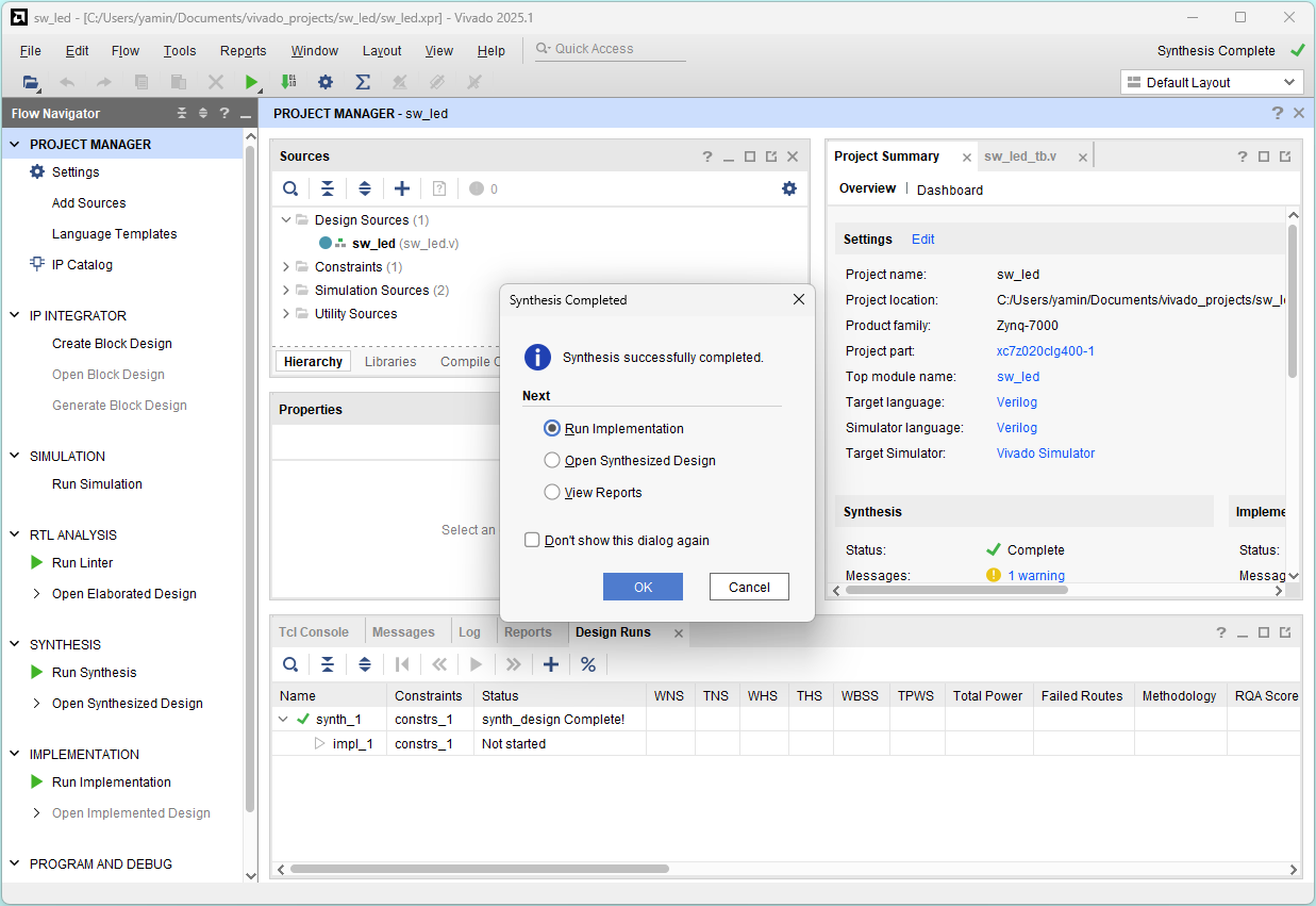
Run synthesis
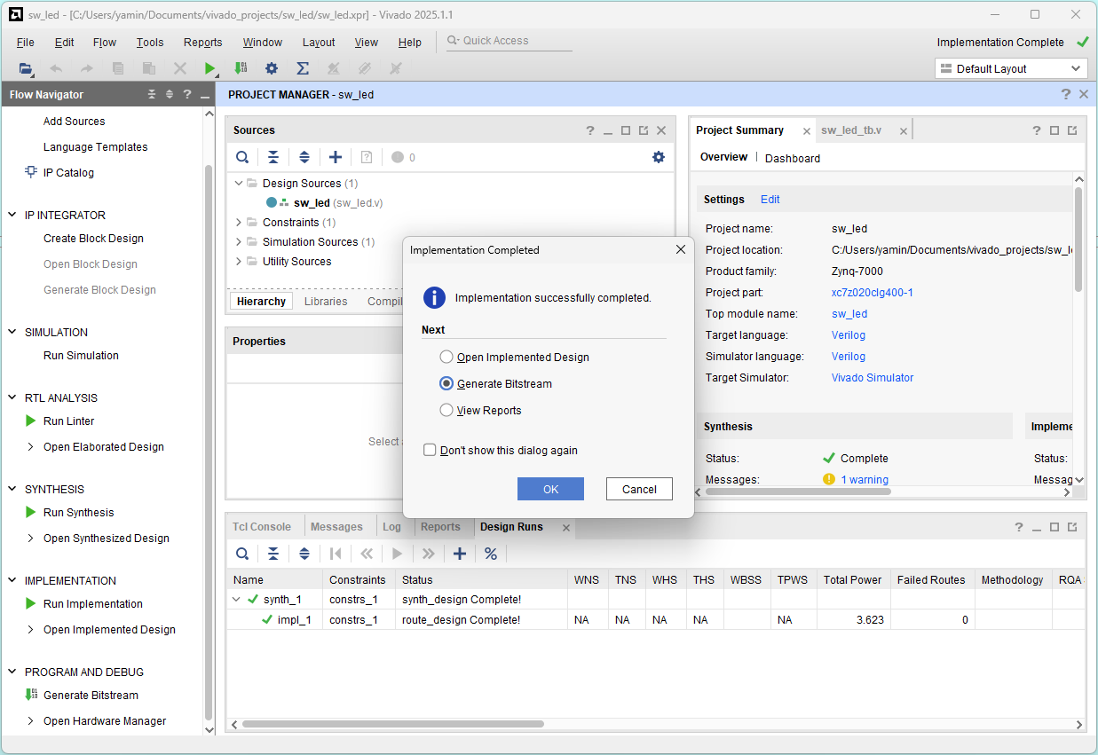
Click Run Synthesis and click OK
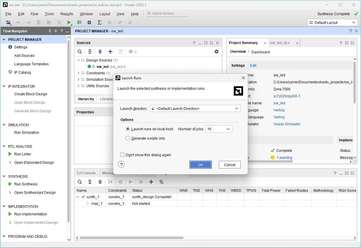
Run implementation
Click OK (Run Implementation)
Click OK
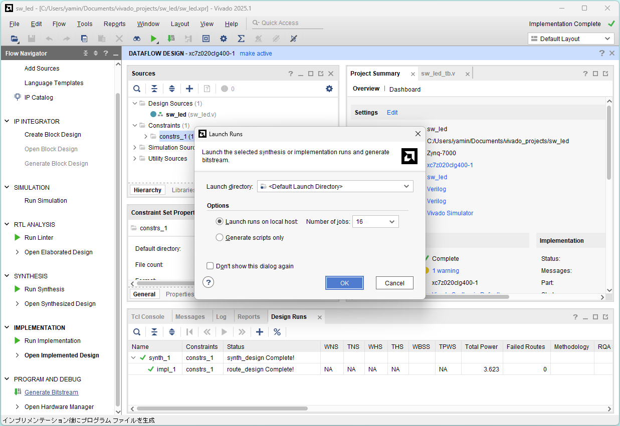
Generate bitstream
Select Generate Bitstream and click OK
Click OK
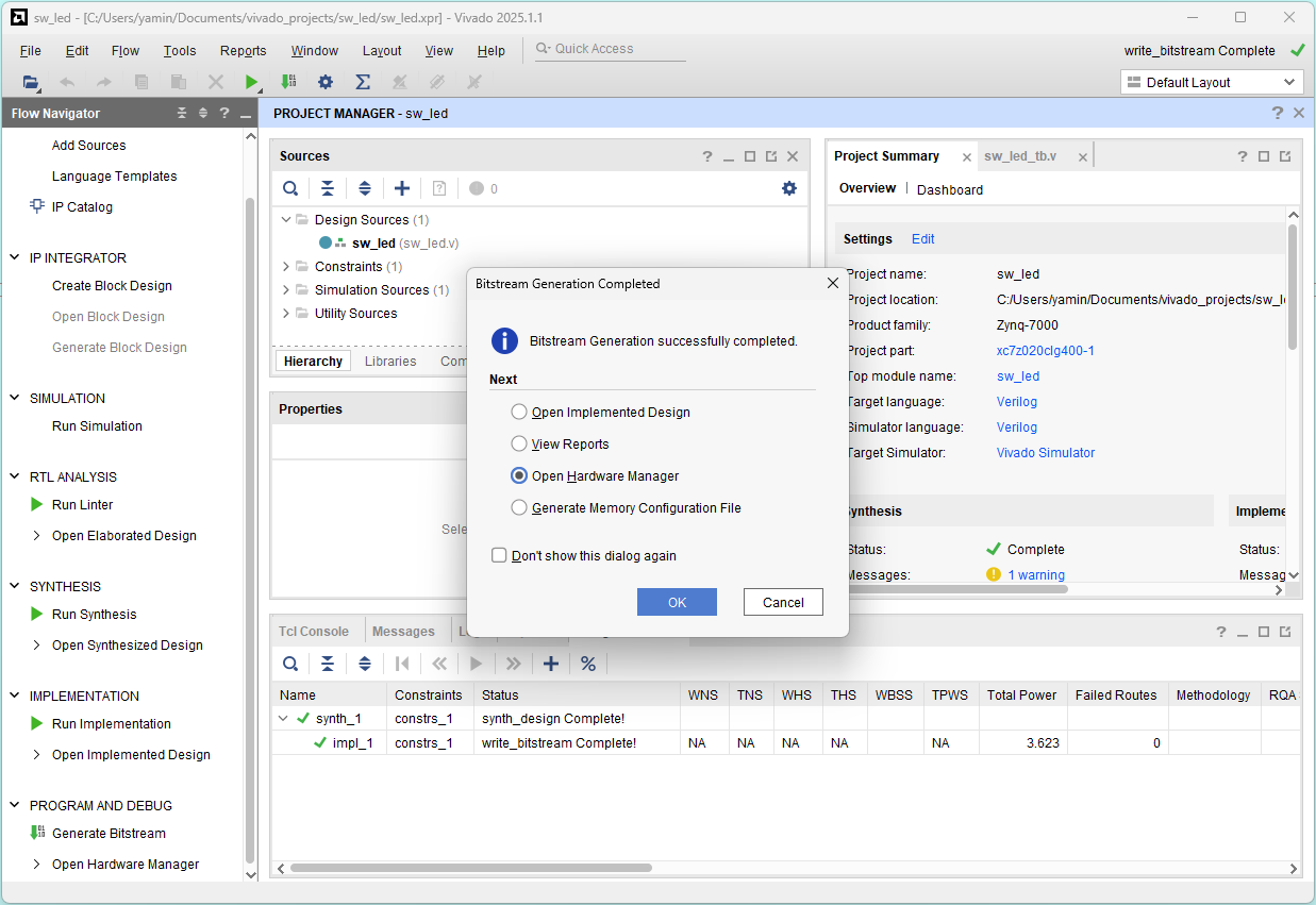
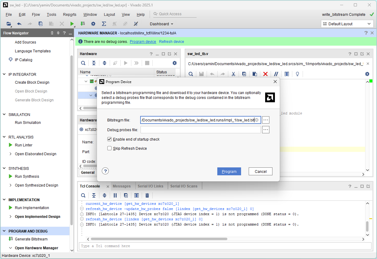
Program device
Select Open Hardware Manager and click OK
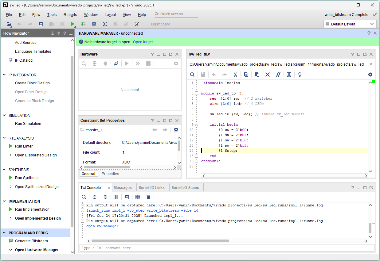
No hardware target is open. Click Open target
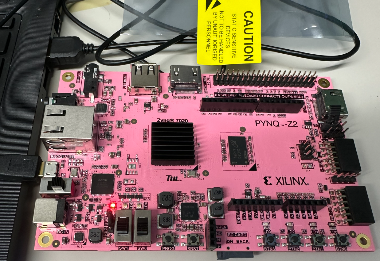
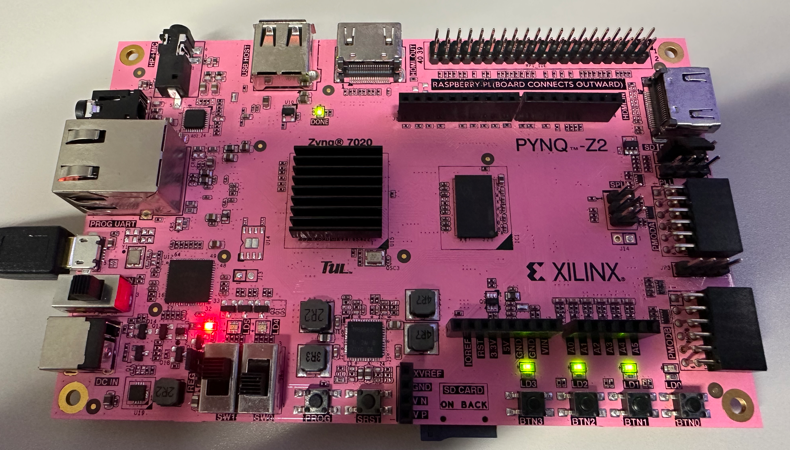
Connect PYNQ-Z2 board to PC and power on the board
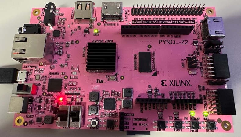
Click Program device and click Program
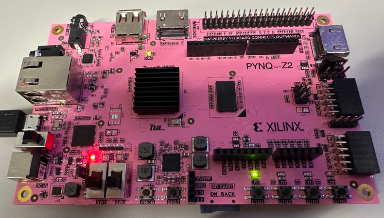
b = 0, a = 0 (sw[1] = 0, sw[0] = 0)
`timescale 1ns/1ns

module sw_led (
    input  [1:0] sw, // 2 switches
    output [3:0] led // 4 LEDs
  );

  assign led[0] = sw[1] & sw[0]; // b AND a
  assign led[1] = sw[1] | sw[0]; // b  OR a
  assign led[2] = sw[1] ^ sw[0]; // b XOR a
  assign led[3] =        ~sw[0]; //   NOT a
endmodule
led[0] = 0 & 0 = 0
led[1] = 0 | 0 = 0
led[2] = 0 ^ 0 = 0
led[3] =    ~0 = 1
b = 0, a = 1 (sw[1] = 0, sw[0] = 1)
`timescale 1ns/1ns

module sw_led (
    input  [1:0] sw, // 2 switches
    output [3:0] led // 4 LEDs
  );

  assign led[0] = sw[1] & sw[0]; // b AND a
  assign led[1] = sw[1] | sw[0]; // b  OR a
  assign led[2] = sw[1] ^ sw[0]; // b XOR a
  assign led[3] =        ~sw[0]; //   NOT a
endmodule
led[0] = 0 & 1 = 0
led[1] = 0 | 1 = 1
led[2] = 0 ^ 1 = 1
led[3] =    ~1 = 0
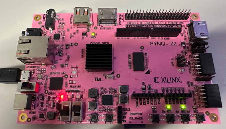
1 = 0, a = 0 (sw[1] = 1, sw[0] = 0)
`timescale 1ns/1ns

module sw_led (
    input  [1:0] sw, // 2 switches
    output [3:0] led // 4 LEDs
  );

  assign led[0] = sw[1] & sw[0]; // b AND a
  assign led[1] = sw[1] | sw[0]; // b  OR a
  assign led[2] = sw[1] ^ sw[0]; // b XOR a
  assign led[3] =        ~sw[0]; //   NOT a
endmodule
led[0] = 1 & 0 = 0
led[1] = 1 | 0 = 1
led[2] = 1 ^ 0 = 1
led[3] =    ~0 = 1
b = 1, a = 1 (sw[1] = 1, sw[0] = 1)
`timescale 1ns/1ns

module sw_led (
    input  [1:0] sw, // 2 switches
    output [3:0] led // 4 LEDs
  );

  assign led[0] = sw[1] & sw[0]; // b AND a
  assign led[1] = sw[1] | sw[0]; // b  OR a
  assign led[2] = sw[1] ^ sw[0]; // b XOR a
  assign led[3] =        ~sw[0]; //   NOT a
endmodule
led[0] = 1 & 1 = 1
led[1] = 1 | 1 = 1
led[2] = 1 ^ 1 = 0
led[3] =    ~1 = 0
Power off the board and close the Vivado program
File -> Exit
Summary of design flow
- Build a project
- Project name and location
- Project Verilog HDL files (.v)
- Project constraint file (.xdc)
- Project device (Zynq-7000 xc7z020clg400-1)
- Functional simulation
- Project testbench file (_tb.v)
- Run simulation
- Check and save waveform file
- Run synthesis
- Run implementation
- Generate bitsteam
- Program device