Styles of Verilog HDL
Three styles:
- Structural style (構造記述)
- Dataflow style (データフロー記述)
- Behavioral style (機能記述)
Style 1 is likely a hardware design and Style 3 is likely a software design.
Full adder design in three styles
Full adder signals
input  a, b; // two inputs a and b
input  ci;   // carry in
output s;    // sum
output co;   // carry out
Full adder truth table
| Input | Output | Comment | |||
| a | b | ci | co | s | a + b + ci = co s |
| 0 | 0 | 0 | 0 | 0 | 0 + 0 + 0 = 0 0 |
| 0 | 0 | 1 | 0 | 1 | 0 + 0 + 1 = 0 1 |
| 0 | 1 | 0 | 0 | 1 | 0 + 1 + 0 = 0 1 |
| 0 | 1 | 1 | 1 | 0 | 0 + 1 + 1 = 1 0 |
| 1 | 0 | 0 | 0 | 1 | 1 + 0 + 0 = 0 1 |
| 1 | 0 | 1 | 1 | 0 | 1 + 0 + 1 = 1 0 |
| 1 | 1 | 0 | 1 | 0 | 1 + 1 + 0 = 1 0 |
| 1 | 1 | 1 | 1 | 1 | 1 + 1 + 1 = 1 1 |
Full adder logic expressions
$s=\overline{a}\ \overline{b}\ ci + \overline{a}\ b\ \overline{ci} + a\ \overline{b}\ \overline{ci} + a\ b\ ci = a \oplus b \oplus ci$
$co=\overline{a}\ b\ ci + a\ \overline{b}\ ci + a\ b\ \overline{ci} + a\ b\ ci = a\ b + b\ ci + ci\ a$
Full adder schematic

Full adder in structural style (構造記述)
Same as the schematic. "xor", "and", and "or" are names of logic gates. A name of wire type is given to an internal wire in schematic, such as "ab", "bc", and "ca" in the example.
1 2 3 4 5 6 7 8 9 10 |
module full_adder_structural (a, b, ci, s, co); // full adder, structural style input a, b, ci; // inputs: a, b, carry_in output s, co; // outputs: sum, carry_out wire ab, bc, ca; // wires, outputs of and gates xor i1 (s, a, b, ci); // xor (out, in1, in2, in3); and i2 (ab, a, b); // and (out, in1, in2); and i3 (bc, b, ci); // and (out, in1, in2); and i4 (ca, ci, a); // and (out, in1, in2); or i5 (co, ab, bc, ca); // or (out, in1, in2, in3); endmodule |
Testbench for simulation:
1 2 3 4 5 6 7 8 9 10 11 12 13 14 15 |
`timescale 1ns/1ns
module full_adder_structural_tb;
    reg  a, b, ci;
    wire s, co;

    full_adder_structural inst (a, b, ci, s, co);

    initial begin
        #0 a = 0; b = 0; ci = 0;
        #8 $stop;
    end
    always #1  a = ~a;
    always #2  b = ~b;
    always #4 ci = ~ci;
endmodule
|
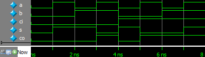
Simulation waveform:
Full adder in dataflow style (データフロー記述)
Same as the logic expressions. "^", "&", and "|" denote XOR, AND, and OR operations, respectively.
1 2 3 4 5 6 |
module full_adder_dataflow(a, b, ci, s, co); // full adder, dataflow style input a, b, ci; // inputs: a, b, carry_in output s, co; // outputs: sum, carry_out assign s = a ^ b ^ ci; // sum of inputs assign co = a & b | b & ci | ci & a; // carry_out endmodule |
Full adder in behavioral style (機能記述)
Focus on What We Want (WWW) which is a sum of three inputs; therefore we perform the addition operation. {co,s} has two bits. You can see that, this style does not concern the implementation details of the hardware circuit.
1 2 3 4 5 |
module full_adder_behavioral (a, b, ci, s, co); // full adder, behavioral style input a, b, ci; // inputs: a, b, carry_in output s, co; // outputs: sum, carry_out assign {co,s} = a + b + ci; // two-bit {co,s} output endmodule |
Exercise
Design and simulate the following circuit (multiplexer) in three Verilog HDL styles, and implement dataflow style version on FPGA.

Structural style (構造記述)
1 2 3 4 5 6 7 8 9 10 11 12 13 |
module switch_button_mux2x1_struct (
    input  A, B, SEL, // SEL: Select
    output Y
  );

  wire , , ;      // 3 wires

  not i1 (  , SEL);  // not (output, input)
  and i2 (  ,  , A); // and (output, input1, input2)
  and i3 (  ,  , B); // and (output, input1, input2)
  or  i4 ( Y,  ,  ); // or  (output, input1, input2)

endmodule
|
Write the testbench module switch_button_mux2x1_struct_tb.v, compile it and do the simulation with ModelSim.
Dataflow style (データフロー記述)
1 2 3 4 5 6 7 8 |
module switch_button_mux2x1_dataflow (
    input  A, B, SEL, // SEL: Select
    output Y
  );

  assign Y = ; // logic expression

endmodule
|
Write the testbench module switch_button_mux2x1_dataflow_tb.v, compile it and do the simulation with ModelSim, and implement it on FPGA.
Behavioral style (機能記述)
1 2 3 4 5 6 7 8 |
module switch_button_mux2x1_behavior (
    input  A, B, SEL, // SEL: Select
    output Y
  );

  assign Y = SEL ? B : A; // if (SEL == 1) Y = B; else Y = A;

endmodule
|
Write the testbench module switch_button_mux2x1_behavior_tb.v, compile it and do the simulation with ModelSim.