A simple circuit
Design the following circuit in Verilog HDL and implement it on DE0-CV FPGA board.

Implementation on DE0-CV with Quartus II
Step 0: Create a folder C:\Users\admin\Documents\projects.
Step 1: Start Altera - Quartus II 13.1. If Quartus II 13.1 was not installed on your PC, download it from either CIS Storage Server or Intel FPGA Software Download Center and install it.
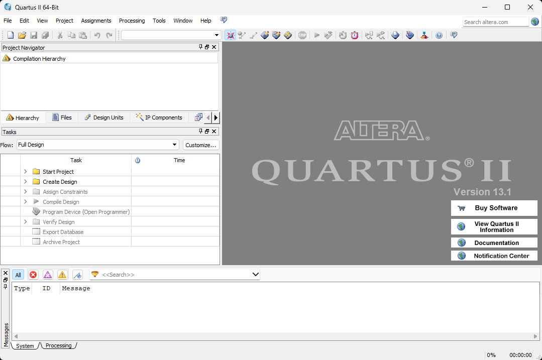
Step 2: In Quartus II, File - New Project Wizard.
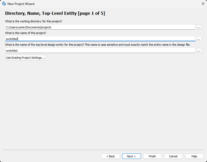
Step 3: Set working directory to C:\Users\admin\Documents\projects.
Step 4: Set the name of the project to switchled.
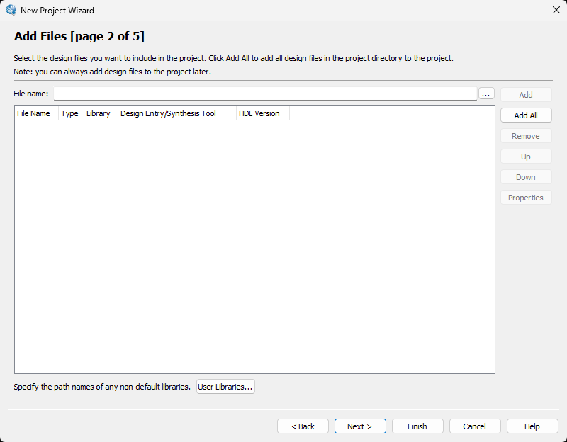
Step 5: If switchled.v exists, add file switchled.v (only switchled.v. The switchled_tb.v is just for simulation with ModelSim).
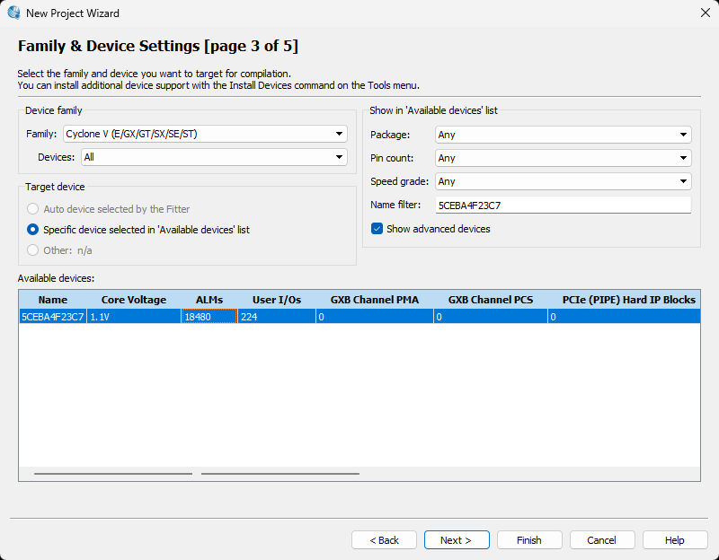
Step 6: Set device to Cyclone V - 5CEBA4F23C7(FPGA chip in DE0-CV board).
Step 7: Click Finish.
Step 8: Create file switchled.v.
File - New - Verilog HDL File - OK
Add the following to the editor window and save it to switchled.v.
Project - Add current File to Project
1 2 3 4 5 6 7 8 9 10 11 |
module switchled ( input [1:0] sw, // 2 switches output [3:0] led // 4 LEDs ); assign led[0] = sw[1] & sw[0]; // b AND a assign led[1] = sw[1] | sw[0]; // b OR a assign led[2] = ~sw[0]; // NOT a assign led[3] = ~sw[1]; // NOT b endmodule |
Step 9: In Quartus II, Ctrl+k (analysis and synthesis).
Step 10: In Quartus II, Assignments - Pin Planner.
Step 11: Referring to User Manual, assign pins as below (set pin names in Location column).
Ex. pin_name of LED[0] is PIN_AA2 (See Table 3-3 and Table 3-4 of P24 and P25 in User Manual).
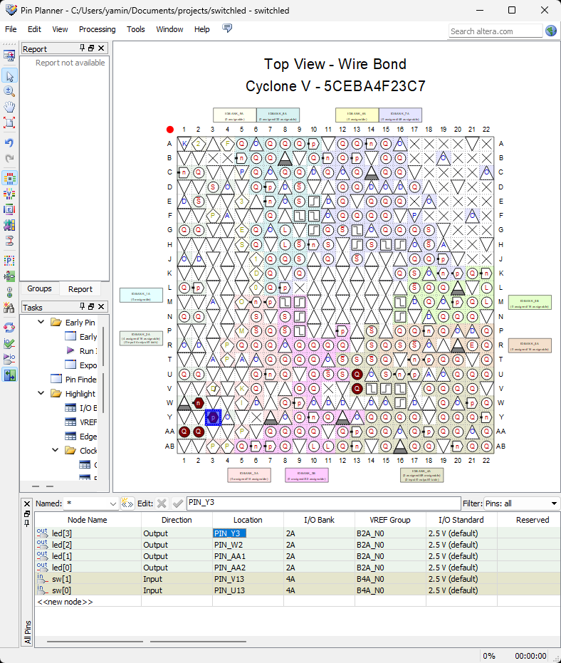
Or add the following to switchled.qsf.
set_location_assignment PIN_U13 -to sw[0]
set_location_assignment PIN_V13 -to sw[1]
set_location_assignment PIN_AA2 -to led[0]
set_location_assignment PIN_AA1 -to led[1]
set_location_assignment PIN_W2 -to led[2]
set_location_assignment PIN_Y3 -to led[3]
Step 12: In Quartus II, Ctrl+l (full compile).
Step 13: Connect DE0-CV board to your PC with Type A to B USB Cable.
Step 14: Push Red Button to power on DE0-CV board. No need to use AC adaptor; the power is suplied by USB.
Install USB-Blaster Driver (only one time, steps 14 - 18):
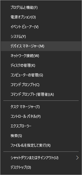
Step 15: Start Device Manager (right-click Win10 Start Button or Win+x).
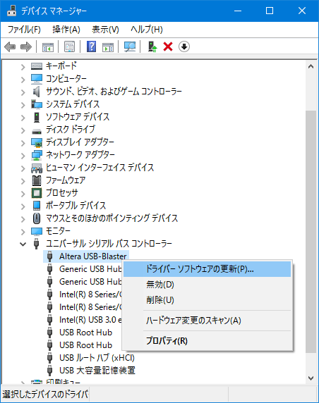
Step 16: Update Altera USB-Blaster Driver (right-click). Note that it may appear in a different place.
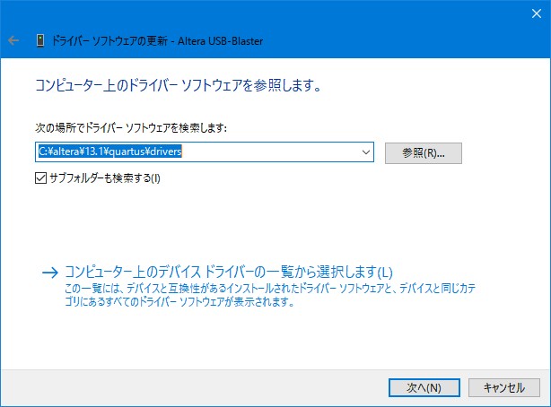
Step 17: Find the driver in this PC.
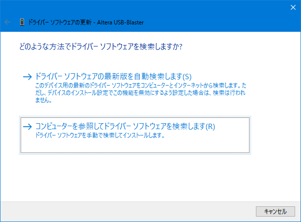
Step 18: Input driver path C:\altera\13.1\quartus\drivers and then click Next. Note that the driver may be in a different place in your PC, for example, in C:\Software\quartus\quartus\drivers.
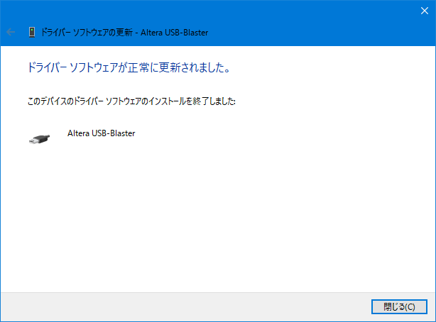
Step 19: Installed.
Step 20: In Quartus II, Tools - Programmer.
Step 21: Hardware Setup: select USB-Blaster.
Step 22: Click Start button to program FPGA Chip. In case there is no file name displied, click Add File button to load output_files/switchled.sof.
Step 23: On DE0-CV board, switch sw[0] and sw[1] to see the changes of LEDs.
1 2 3 4 5 6 7 8 9 10 11 |
module switchled ( input [1:0] sw, // 2 switches output [3:0] led // 4 LEDs ); assign led[0] = sw[1] & sw[0]; // b AND a assign led[1] = sw[1] | sw[0]; // b OR a assign led[2] = ~sw[0]; // NOT a assign led[3] = ~sw[1]; // NOT b endmodule |
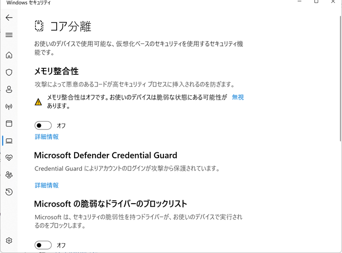
Step 20: Hardware Setup: If there is no USB-Blaster
Windows 11: Start --> 設定 --> プライバシーとセキュリティ --> Windows セキュリティ --> デバイス セキュリティ --> コア分離の詳細 --> メモリ整合性: オフ --> PCを再起動
Exercise
Design the following circuit in Verilog HDL and implement it on DE0-CV FPGA board.

- First, create a new project with the project name "switch_button_mux2x1". Note that we do not create a new folder for it. All projects share the same "projects" folder.
- Referring to the figure above, complete and compile the following Verilog HDL code with ModelSim. The file name is switch_button_mux2x1.v.
1
2
3
4
5
6
7
8
module switch_button_mux2x1 ( input A, B, SEL, // SEL: Select output Y ); // assign Y = ...; endmodule - Implement switch_button_mux2x1.v on the FPGA board (using two buttons and a switch as inputs and a LED as output).
Pin assignments:set_location_assignment PIN_U13 -to SEL set_location_assignment PIN_U7 -to A set_location_assignment PIN_W9 -to B set_location_assignment PIN_AA2 -to Y