A simple circuit
Design the following circuit in Verilog HDL and simulate it with ModelSim.

Design and simulation with ModelSim
If Altera Quartus II 13.1 was not installed on your PC, please download https://storage.cis.k.hosei.ac.jp/pub/CISOnly/QuartusII/13.1/Quartus-web-13.1.0.162-windows.zip and install it on your PC.
Step 1: Create a folder C:\Users\admin\Documents\projects.
Step 2: Start ModelSim.
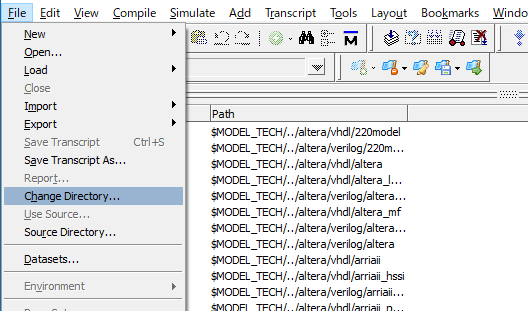
Step 3: In ModelSim, File - Change Directory to C:\Users\admin\Documents\projects.
Step 4: In ModelSim, File - New - Source - Verilog and add the following Verilog HDL codes to edit window (Do NOT use Japanese).
1 2 3 4 5 6 7 8 9 10 11 12 13 14 15 16 |
module sw_led (
    input  [1:0] sw, // 2 switches
    output [9:0] led // 10 LEDs
  );

  assign led[0] =   sw[1]  & sw[0];  //      b  AND a
  assign led[1] = ~(sw[1]  & sw[0]); // NOT (b  AND a)
  assign led[2] =   sw[1]  | sw[0];  //      b   OR a
  assign led[3] = ~(sw[1]  | sw[0]); // NOT (b   OR a)
  assign led[4] =   sw[1]  ^ sw[0];  //      b  XOR a
  assign led[5] = ~(sw[1]  ^ sw[0]); // NOT (b  XOR a)
  assign led[6] =          ~ sw[0];  // NOT         a
  assign led[7] = ~ sw[1];           // NOT  b
  assign led[8] =   sw[1] ~^ sw[0];  //      b NXOR a
  assign led[9] = ~(sw[1] ~^ sw[0]); // NOT (b NXOR a)
endmodule
|
Step 5: In ModelSim, Control_S, save to sw_led.v.
Step 6: In ModelSim, Compile sw_led.v; click Yes to create "work" library.
Step 7: Similarly, create a file sw_led_tb.v (Test Bench - for simulation) and add the following Verilog HDL codes to it. The codes will be explained late.
1 2 3 4 5 6 7 8 9 10 11 12 13 14 15 |
`timescale 1ns/1ns module sw_led_tb; reg [1:0] sw; // 2 switches wire [9:0] led; // 10 LEDs sw_led swled (sw, led); // invoke sw_led module initial begin #0 sw = 2'b00; #1 sw = 2'b01; #1 sw = 2'b10; #1 sw = 2'b11; #1 $stop; end endmodule |
Step 8: In ModelSim, Compile sw_led_tb.v.
Step 9: In ModelSim, Simulate work.sw_led_tb.
Step 10: In Transcript window, execute
add wave /*
Step 11: In Transcript window, execute
run
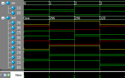
Step 12: Select Wave window and adjust the waveform, you can see the waveforms as below.
For ease of checking, re-show sw_led.v.
1 2 3 4 5 6 7 8 9 10 11 12 13 14 15 |
module sw_led (
    input  [1:0] sw, // 2 switches
    output [9:0] led // 10 LEDs
  );
  assign led[0] =   sw[1]  & sw[0];  //      b  AND a
  assign led[1] = ~(sw[1]  & sw[0]); // NOT (b  AND a)
  assign led[2] =   sw[1]  | sw[0];  //      b   OR a
  assign led[3] = ~(sw[1]  | sw[0]); // NOT (b   OR a)
  assign led[4] =   sw[1]  ^ sw[0];  //      b  XOR a
  assign led[5] = ~(sw[1]  ^ sw[0]); // NOT (b  XOR a)
  assign led[6] =          ~ sw[0];  // NOT         a
  assign led[7] = ~ sw[1];           // NOT  b
  assign led[8] =   sw[1] ~^ sw[0];  //      b NXOR a
  assign led[9] = ~(sw[1] ~^ sw[0]); // NOT (b NXOR a)
endmodule
|
Question 1: Check the waveforms of led[7:0].
Question 2: Explain why led[8] = led[5] (in red color) and led[9] = led[4] (in yellow color).
Question 3: Explain the meanings of led values 1ea, 296, 256, and 125, in the waveform.
Verilog HDL modules
HDL --- Hardware Description Languages
- Verilog HDL
- IEEE Standard 1364-1995 (Verilog-1995)
- IEEE Standard 1364-2001 (Verilog-2001)
- VHDL --- VHSIC HDL
- IEEE Standard 1076-1987
- AHDL --- Altera HDL
- ABEL --- Advanced Boolean Expression Language
- SystemVerilog HDL
- IEEE Standard 1800-2005
- SystemC
A regular module
1 2 3 4 5 6 7 8 9 10 11 12 13 14 15 |
module sw_led (
    input  [1:0] sw, // 2 switches
    output [9:0] led // 10 LEDs
  );
  assign led[0] =   sw[1]  & sw[0];  //      b  AND a
  assign led[1] = ~(sw[1]  & sw[0]); // NOT (b  AND a)
  assign led[2] =   sw[1]  | sw[0];  //      b   OR a
  assign led[3] = ~(sw[1]  | sw[0]); // NOT (b   OR a)
  assign led[4] =   sw[1]  ^ sw[0];  //      b  XOR a
  assign led[5] = ~(sw[1]  ^ sw[0]); // NOT (b  XOR a)
  assign led[6] =          ~ sw[0];  // NOT         a
  assign led[7] = ~ sw[1];           // NOT  b
  assign led[8] =   sw[1] ~^ sw[0];  //      b NXOR a
  assign led[9] = ~(sw[1] ~^ sw[0]); // NOT (b NXOR a)
endmodule
|
module and endmodule: keyword, begin and end of a module.
sw_led: module name, must be the same as the file name.
input and output: keywords, define input and output signals.
[1:0] and [9:0]: number of bits. [1:0] - 2 bits: sw[1] and sw[0]; [9:0] - 10 bits: led[9], led[8], led[7], led[6], led[5], led[4], led[3], led[2], led[1], and led[0].
assign: keyword, assign a value to a signal.
&: operator AND.
|: operator OR.
^: operator XOR (Exclusive OR).
~: operator NOT.
//: comment (do NOT use Japanese).
Priority: ~ > & > |
The module can be also written in the following format (try to find the differences).
module sw_led (sw, led);
  input  [1:0] sw;  // 2 switches
  output [9:0] led; // 10 LEDs
  ...
endmodule
A test bench module
1 2 3 4 5 6 7 8 9 10 11 12 13 14 15 |
`timescale 1ns/1ns module sw_led_tb; reg [1:0] sw; // 2 switches wire [9:0] led; // 10 LEDs sw_led swled (sw, led); // invoke sw_led module initial begin #0 sw = 2'b00; #1 sw = 2'b01; #1 sw = 2'b10; #1 sw = 2'b11; #1 $stop; end endmodule |
This is a module for simulation (test bench). It has no input/output signal.
`timescale 1ns/1ns: the first 1ns defines time unit and the second 1ns defines the minimum time precision we can use in the simulation.
reg: the type of sw. With reg (register) type, sw can be assigned with different values several times.
wire: the type of led.
sw_led swled (sw, led): invoke sw_led module; swled: instance name; (sw, led): parameters for sw_led module.
initial: a block that describes the behaviors of signal sw.
#: the time mark that describes the time delay in the unit of nanoseconds (ns).
2'b00: 2': two bits; b: 00 is a binary number (d: decimal; h: hexadecimal).
$stop: stop simulation.
Exercise
Design the following circuit in Verilog HDL and simulate it with ModelSim.

- Referring to the figure above, complete and compile the following Verilog HDL code with ModelSim. The file name is switch_button_mux2x1.v.
1
2
3
4
5
6
7
8
module switch_button_mux2x1 ( input A, B, SEL, // SEL: Select output Y ); // assign Y = ...; endmodule - Write the testbench module switch_button_mux2x1_tb.v, compile it and do the simulation with ModelSim.
- Show your codes and waveform.
- Implement it on FPGA.